Design Services:
GaN MMIC
CML Micro has experience of designing GaN MMICs using the 0.25µm GaN-on-SiC processes of GCS, MACOM (formerly Wolfspeed), Qorvo, UMS, WIN Semiconductors. Our design activity has included Doherty PAs for sub-6GHz 5G, compact X-band PAs for phased array radar, very high linearity (high power handling) microwave switching functions, robust GaN LNAs, broadband GaN PA MMICs for ESM applications, and high linearity GaN PAs for point to point link applications.
GaN MMIC Design Examples
28GHz Doherty GaN PA
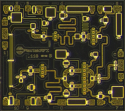 This Doherty PA is designed for the 28GHz 5G frequency band using the 0.15µm G28v5 GaN-on-SiC process from MACOM (formerly Wolfspeed). An asymmetrical Doherty topology improves efficiency at backed-off power levels. RFOW measured gain was 20dB with a peak output power of 35dBm and a PAE at 8dB back-off (27dBm RF output power) of 19%.
Read a technical paper about the design of the 28GHz Doherty GaN PA
15GHz GaN PA
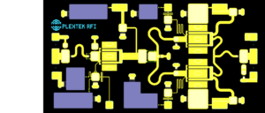
This 15GHz GaN PA for point-to-point links uses MACOM’s 0.25µm GaN on SiC process, and offers an output power of 38dBm with an output IP3 of > 46dBm in a small die size.
View a video about the design of this PA
Read a technical paper about the design of the 15GHz GaN PA
3.5GHz GaN PA
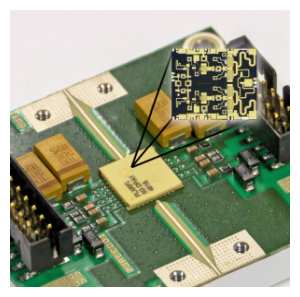
This image shows a connectorised evaluation PCB for a fully integrated 3.5GHz Doherty PA designed on GCS’ 0.4µm GaN on SiC process. The IC is housed in a laminate QFN package demonstrated, it can provide a Psat of 45dBm with a peak PAE of 50%. The Doherty architecture allows a PAE of 31.5% to be achieved at 8dB power back-off.
View a video about the design of this PA
Read a technical paper about this design
X-band GaN PA for Phased Array Radar
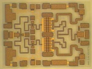
This X-band GaN PA MMIC for phased array radar applications covers 9 to 11.5GHz. It has an output power of 7W (38.5dBm) from a 29dBm drive with a Power Added Efficiency (PAE) of 42% and a die size is just 1.5mm x 2mm (allowing around 2,300 PAs to be fabricated on a single 4” diameter wafer). The design was realised on the 0.25µm gate length GaN on SiC process of UMS (GH25).
Watch a technical tutorial video describing the design of this X-band GaN PA MMIC
Read our technical paper “An X-band GaN PA MMIC for Phased Array Radar”
We have also designed a number of GaN MMIC functional blocks for which we own the IP. This library of GaN MMIC IP can be used to help develop custom GaN ICs for our clients with reduced risk and timescales.
Technical publications describing some of the other GaN MMIC IP developed by CML Micro Design Services are available using the links below:
CML Micro has designed GaN MMICs on the world’s leading foundries, including GCS, MACOM (formerly Wolfspeed), Qorvo, UMS and WIN Semiconductor.
To discuss how CML Micro could develop GaN MMICs for you, please email designservices@cmlmicro.com